- 您现在的位置:买卖IC网 > Sheet目录338 > LTC3220EPF#PBF (Linear Technology)IC LED DRVR QVGA DISPLAY 28UTQFN
�� �
�
�LTC3220/LTC3220-1�
�OPERATION�
�sub-address� register� is� then� written� to,� followed� by� the�
�data� register.� Each� data� register� has� a� sub-address.� After�
�the� data� register� has� been� written� a� load� pulse� is� created�
�after� the� stop� bit.� The� load� pulse� transfers� all� of� the� data�
�held� in� the� data� registers� to� the� DAC� registers.� The� stop�
�bit� can� be� delayed� until� all� of� the� data� master� registers�
�have� been� written.� At� this� point� the� LED� current� will� be�
�changed� to� the� new� settings.� The� serial� port� uses� static�
�logic� registers� so� there� is� no� minimum� speed� at� which� it�
�can� be� operated.�
�when� the� bus� is� not� in� use.� External� pull-up� resistors� or�
�current� sources,� such� as� the� LTC1694� SMBus� accelerator,�
�are� required� on� these� lines.�
�The� LTC3220/LTC3220-1� are� receive-only� (slave)� devices.�
�There� are� two� I� 2� C� addresses� available.� The� LTC3220� I� 2� C�
�address� is� 0011100� and� the� LTC3220-1� I� 2� C� address� is�
�0011101.� The� I� 2� C� address� is� the� only� difference� between�
�the� LTC3220� and� LTC3220-1.�
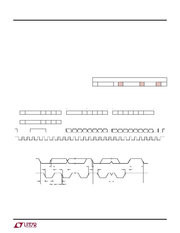
�Write� Word� Protocol� Used� By� the� LTC3220/LTC3220-1�
�I� 2� C� Interface�
�1�
�7�
�1�
�1�
�8�
�1�
�8�
�1�
�1�
�The� LTC3220/LTC3220-1� communicate� with� a� host� (master)�
�using� the� standard� I� 2� C� 2-wire� interface.� The� Timing� Diagram�
�S� Slave� Address� Wr� A� *Sub-Address� A� Data� Byte�
�S� =� Start� Condition,� Wr� =� Write� Bit� =� 0,� A� =� Acknowledge,�
�A�
�P**�
�(Figure� 3)� shows� the� timing� relationship� of� the� signals� on�
�the� bus.� The� two� bus� lines,� SDA� and� SCL,� must� be� high�
�SUB-ADDRESS�
�P� =� Stop� Condition�
�*The� sub-address� uses� only� the� ?rst� 5� bits,� D0,� D1,� D2,� D3� and� D4.�
�**Stop� can� be� delayed� until� all� of� the� data� registers� have� been� written.�
�DATA� BYTE�
�LTC3220�
�ADDRESS�
�WR�
�0�
�0�
�1�
�1�
�1�
�0�
�0�
�0�
�S7�
�S6�
�S5�
�S4�
�S3�
�S2�
�S1�
�S0�
�7�
�6�
�5�
�4�
�3�
�2�
�1�
�0�
�LTC3220-1�
�ADDRESS�
�WR�
�0�
�0�
�1�
�1�
�1�
�0�
�1�
�0�
�START�
�STOP�
�SDA�
�0�
�0�
�1�
�1�
�1�
�0�
�0�
�0�
�ACK�
�S7�
�S6�
�S5�
�S4�
�S3�
�S2�
�S1�
�S0� ACK�
�7�
�6�
�5�
�4�
�3�
�2�
�1�
�0�
�ACK�
�SCL�
�1�
�2�
�3�
�4�
�5�
�6�
�7�
�8�
�9�
�1�
�2�
�3�
�4�
�5�
�6�
�7�
�8�
�9�
�1�
�2�
�3�
�4�
�5�
�6�
�7�
�8�
�9�
�3220� FO2�
�Figure� 2.� Bit� Assignments�
�SDA�
�t� SU,� DAT�
�t� SU,� STA�
�t� BUF�
�t�
�SCL�
�HD,� STA�
�t� LOW�
�t� HIGH�
�t� HD,� DAT�
�t� HD,� STA�
�t� SP�
�t� SU,� STO�
�3220� F03�
�START�
�CONDITION�
�t� r�
�t� f�
�REPEATED� START�
�CONDITION�
�STOP�
�CONDITION�
�START�
�CONDITION�
�Figure� 3.� Timing� Parameters�
�32201fc�
�11�
�发布紧急采购,3分钟左右您将得到回复。
相关PDF资料
LTC3230EUD#PBF
IC LED DRIVR WHITE BCKLGT 20-QFN
LTC3452EUF#TRPBF
IC LED DRIVER PHOTO FLASH 20-QFN
LTC3453EUF#TRPBF
IC LED DRIVER PHOTO FLASH 16-QFN
LTC3454EDD#TRPBF
IC LED DRIVER PHOTO FLASH 10-DFN
LTC3490EDD#PBF
IC LED DRIVER PHOTO FLASH 8-DFN
LTC3783EFE#PBF
IC LED DRVR PWM CONTROL 16-TSSOP
LV5026MC-AH
IC LED DRIVER 1CH HV 10SOIC
LV5213LP-TE-L-E
IC LED DVR 3CH CELL PHONE VCT16
相关代理商/技术参数
LTC3220EPF#TRPBF
功能描述:IC LED DRVR QVGA DISPLAY 28UTQFN RoHS:是 类别:集成电路 (IC) >> PMIC - LED 驱动器 系列:- 标准包装:6,000 系列:- 恒定电流:- 恒定电压:- 拓扑:开路漏极,PWM 输出数:4 内部驱动器:是 类型 - 主要:LED 闪烁器 类型 - 次要:- 频率:400kHz 电源电压:2.3 V ~ 5.5 V 输出电压:- 安装类型:表面贴装 封装/外壳:8-VFDFN 裸露焊盘 供应商设备封装:8-HVSON 包装:带卷 (TR) 工作温度:-40°C ~ 85°C 其它名称:935286881118PCA9553TK/02-TPCA9553TK/02-T-ND
LTC3220EPF-1#PBF
功能描述:IC LED DRVR QVGA DISPLAY 28UTQFN RoHS:是 类别:集成电路 (IC) >> PMIC - LED 驱动器 系列:- 标准包装:6,000 系列:- 恒定电流:- 恒定电压:- 拓扑:开路漏极,PWM 输出数:4 内部驱动器:是 类型 - 主要:LED 闪烁器 类型 - 次要:- 频率:400kHz 电源电压:2.3 V ~ 5.5 V 输出电压:- 安装类型:表面贴装 封装/外壳:8-VFDFN 裸露焊盘 供应商设备封装:8-HVSON 包装:带卷 (TR) 工作温度:-40°C ~ 85°C 其它名称:935286881118PCA9553TK/02-TPCA9553TK/02-T-ND
LTC3220EPF-1#TRPBF
功能描述:IC LED DRVR QVGA DISPLAY 28UTQFN RoHS:是 类别:集成电路 (IC) >> PMIC - LED 驱动器 系列:- 标准包装:6,000 系列:- 恒定电流:- 恒定电压:- 拓扑:开路漏极,PWM 输出数:4 内部驱动器:是 类型 - 主要:LED 闪烁器 类型 - 次要:- 频率:400kHz 电源电压:2.3 V ~ 5.5 V 输出电压:- 安装类型:表面贴装 封装/外壳:8-VFDFN 裸露焊盘 供应商设备封装:8-HVSON 包装:带卷 (TR) 工作温度:-40°C ~ 85°C 其它名称:935286881118PCA9553TK/02-TPCA9553TK/02-T-ND
LTC3220EPF-1-PBF
制造商:LINER 制造商全称:Linear Technology 功能描述:360mA Universal 18-Channel LED Driver
LTC3220EPF-1-TRPBF
制造商:LINER 制造商全称:Linear Technology 功能描述:360mA Universal 18-Channel LED Driver
LTC3220EPFPBF
制造商:Linear Technology 功能描述:360mA 18-Channel LED Driver LTC3220EPF
LTC3220EPF-PBF
制造商:LINER 制造商全称:Linear Technology 功能描述:360mA Universal 18-Channel LED Driver
LTC3220EPF-TRPBF
制造商:LINER 制造商全称:Linear Technology 功能描述:360mA Universal 18-Channel LED Driver